
大神们,请教一下,我在LS1046单板(ARM A72)调试MMU,按如下配置创建页表,我把下面4个1G空间都映射到第1个1G的物理地址上,我会在0x10010000的SRAM地址上写数据来check结果,但是发现从T32上看,映射关系都是对的,而实际上0x40000000段或者有时是0xC0000000段总是没有映射过去
如图: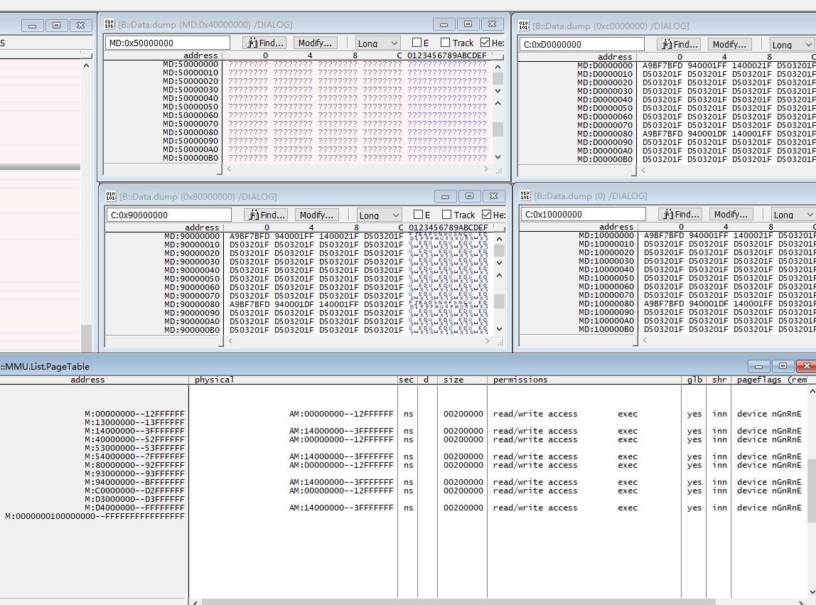
4段地址空间的映射关系:
00000000--3FFFFFFF --> 00000000--3FFFFFFF
40000000--7FFFFFFF --> 00000000--3FFFFFFF
80000000--BFFFFFFF --> 00000000--3FFFFFFF
C0000000--FFFFFFFF --> 00000000--3FFFFFFF
来自Trace32的MMU.List.PageTable如下:
__________________address________________|_physical______________________|sec|_d_|_size____|_permissions_______ _____|_glb|_shr|_pageflags_(remapped)|
                     M:00000000--12FFFFFF|          AM:00000000--12FFFFFF| ns|   | 00200000| read/write access  exec | yes| inn| device nGnRnE       |
                     M:13000000--13FFFFFF|                               |   |   |         |                         |    |    |                     |
                     M:14000000--3FFFFFFF|          AM:14000000--3FFFFFFF| ns|   | 00200000| read/write access  exec | yes| inn| device nGnRnE       |
                     M:40000000--52FFFFFF|          AM:00000000--12FFFFFF| ns|   | 00200000| read/write access  exec | yes| inn| device nGnRnE       |
                     M:53000000--53FFFFFF|                               |   |   |         |                         |    |    |                     |
                     M:54000000--7FFFFFFF|          AM:14000000--3FFFFFFF| ns|   | 00200000| read/write access  exec | yes| inn| device nGnRnE       |
                     M:80000000--92FFFFFF|          AM:00000000--12FFFFFF| ns|   | 00200000| read/write access  exec | yes| inn| device nGnRnE       |
                     M:93000000--93FFFFFF|                               |   |   |         |                         |    |    |                     |
                     M:94000000--BFFFFFFF|          AM:14000000--3FFFFFFF| ns|   | 00200000| read/write access  exec | yes| inn| device nGnRnE       |
                     M:C0000000--D2FFFFFF|          AM:00000000--12FFFFFF| ns|   | 00200000| read/write access  exec | yes| inn| device nGnRnE       |
                     M:D3000000--D3FFFFFF|                               |   |   |         |                         |    |    |                     |
                     M:D4000000--FFFFFFFF|          AM:14000000--3FFFFFFF| ns|   | 00200000| read/write access  exec | yes| inn| device nGnRnE       |
     M:0000000100000000--FFFFFFFFFFFFFFFF|                               |   |   |         |                         |    |    |                     |
代码如下:
.global mmu_init

mmu_init:

// Initialize translation table control registers
LDR X1, =0x3520     // 4GB space 4KB granularity
// Inner-shareable.
MSR TCR_EL3, X1     // Normal Inner and Outer Cacheable.
LDR X1, =0xFF440400     // ATTR0 Device-nGnRnE ATTR1 Device.
MSR MAIR_EL3, X1    // ATTR2 Normal Non-Cacheable.
            // ATTR3 Normal Cacheable.
ADR X0, ttb0_base   // ttb0_base must be a 4KB-aligned address.
MSR TTBR0_EL3, X0
DSB SY
ISB

// Enable caches and the MMU.
MRS X0, SCTLR_EL3
//ORR X0, X0, #(0x1 << 2) // The C bit (data cache).
ORR X0, X0, #(0x1 << 12)  // The I bit (instruction cache).
ORR X0, X0, #0x1          // The M bit (MMU).
MSR SCTLR_EL3, X0
DSB SY
ISB

//for debug
ldr x0, =0xd0010000
ldr x2, [x0]
ldr x1, =0x55555555
str x1, [x0]

ldr x0, =0x10010100
ldr x2, [x0]
ldr x1, =0x55555555
str x1, [x0]
ret


// Put a 64-bit value with little endianness.
.macro PUT_64B high, low
.word \low
.word \high
.endm

// Create an entry pointing to a next-level table.
.macro TABLE_ENTRY PA, ATTR
PUT_64B \ATTR, (\PA) + 0x3
.endm

// Create an entry for a 1GB block.
.macro BLOCK_1GB PA, ATTR_HI, ATTR_LO
PUT_64B \ATTR_HI, ((\PA) & 0xC0000000) | \ATTR_LO | 0x1
.endm

// Create an entry for a 2MB block.
.macro BLOCK_2MB PA, ATTR_HI, ATTR_LO
PUT_64B \ATTR_HI, ((\PA) & 0xFFE00000) | \ATTR_LO | 0x1
.endm

// Create an entry for a 4KB page.
.macro PAGE_4KB PA, ATTR_HI, ATTR_LO
PUT_64B \ATTR_HI, ((\PA) & 0xFFFFF000) | \ATTR_LO | 0x3
.endm


.align 12 // 12 for 4KB granule.
ttb0_base:
TABLE_ENTRY level2_0_pagetable, 0
TABLE_ENTRY level2_0_pagetable, 0
TABLE_ENTRY level2_0_pagetable, 0
TABLE_ENTRY level2_0_pagetable, 0

.align 12 // 12 for 4KB granule.
level2_0_pagetable:
.set ADDR, 0x000 // The current page address.
.rept 0x200
BLOCK_2MB (ADDR << 20), 0, 0x740
.set ADDR, ADDR+2
.endr


