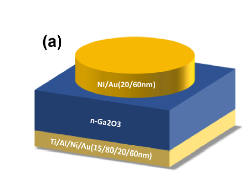
有效载流子密度为1 1017–2 1017 cm 3 。基板厚度约为1mm,尺寸为10×15mm2,Ti/Al/Ni/Au(15 nm/80 20 60 )金属叠层,以在Ti和Ga2O3之间形成欧姆接触。Ni/Au(20 60 )在基板的正面创建了半径为 300 lm 的圆形肖特基阳极电极。
我想用silvaco TCAD重复这个模型,但代码不知怎么写

 分享
分享
晚上好🌙🌙🌙
本答案参考通义千问
在使用 Silvaco TCAD 进行半导体器件仿真时,需要通过 ATLAS 或 DEMO 模块来构建和仿真模型。你提到的结构是一个包含欧姆接触和肖特基电极的 Ga₂O₃ 器件,具体参数如下:
编写一个完整的 Silvaco ATLAS 脚本,用于模拟上述结构,包括:
# 定义Ga2O3基板
material name=Ga2O3
    lattice constant=5.137 angstrom
    dielectric constant=10.0
    mobility model=low field
    bandgap=4.8 eV
    intrinsic carrier concentration=1e-16 cm^-3
    effective mass=0.33
    electron affinity=1.0 eV
end material

# 定义基板尺寸(10mm x 15mm x 1mm)
grid x=10000 y=15000 z=1000
注意: Silvaco 中单位为微米(μm),因此需将毫米转换为微米(1mm = 1000 μm)
# 在基板中注入电子(假设为n型)
doping type=n concentration=1e17 cm^-3
重点: 有效载流子密度范围是 1e17 到 2e17 cm⁻³,可选择中间值或分段设置。
# Ti 层(15nm)
metal name=Ti thickness=15
    contact type=ohmic
    interface material=Ga2O3
    work function=4.0 eV
end metal

# Al 层(80nm)
metal name=Al thickness=80
    contact type=ohmic
    interface material=Ga2O3
    work function=4.0 eV
end metal

# Ni 层(20nm)
metal name=Ni thickness=20
    contact type=schottky
    interface material=Ga2O3
    work function=5.0 eV
end metal

# Au 层(60nm)
metal name=Au thickness=60
    contact type=schottky
    interface material=Ga2O3
    work function=5.0 eV
end metal
重点:
contact type需要根据电极类型进行设置:
ohmic表示欧姆接触(Ti/Ga₂O₃)schottky表示肖特基接触(Ni/Au)
# 定义肖特基阳极电极(直径 600 μm,半径 300 μm)
electrode name=schottky position=x=5000 y=7500 radius=300
    metal=Ni/Au
    contact type=schottky
end electrode

# 定义阴极电极(欧姆接触,覆盖整个基板背面)
electrode name=ohmic position=x=5000 y=7500
    metal=Ti/Al
    contact type=ohmic
    shape=full
end electrode
重点: 使用
shape=full可以让电极覆盖整个基板背面。
# 设置边界条件
boundary condition type=dirichlet
    voltage=0
    electrode=ohmic
end boundary

# 设置求解器参数
solve init
    solver=dc
    max iteration=100
    tolerance=1e-8
end solve
# 输出电流-电压特性
output file=current_volt
    variable=I
    plot=IV
end output

# 输出电势分布
output file=potential
    variable=V
    plot=contour
end output
# 定义材料
material name=Ga2O3
    lattice constant=5.137 angstrom
    dielectric constant=10.0
    mobility model=low field
    bandgap=4.8 eV
    intrinsic carrier concentration=1e-16 cm^-3
    effective mass=0.33
    electron affinity=1.0 eV
end material

# 网格设置(10mm x 15mm x 1mm)
grid x=10000 y=15000 z=1000

# 掺杂设置
doping type=n concentration=1e17 cm^-3

# 金属叠层(Ti/Al/Ni/Au)
metal name=Ti thickness=15
    contact type=ohmic
    interface material=Ga2O3
    work function=4.0 eV
end metal

metal name=Al thickness=80
    contact type=ohmic
    interface material=Ga2O3
    work function=4.0 eV
end metal

metal name=Ni thickness=20
    contact type=schottky
    interface material=Ga2O3
    work function=5.0 eV
end metal

metal name=Au thickness=60
    contact type=schottky
    interface material=Ga2O3
    work function=5.0 eV
end metal

# 电极定义
electrode name=schottky position=x=5000 y=7500 radius=300
    metal=Ni/Au
    contact type=schottky
end electrode

electrode name=ohmic position=x=5000 y=7500
    metal=Ti/Al
    contact type=ohmic
    shape=full
end electrode

# 边界条件
boundary condition type=dirichlet
    voltage=0
    electrode=ohmic
end boundary

# 求解器设置
solve init
    solver=dc
    max iteration=100
    tolerance=1e-8
end solve

# 输出结果
output file=current_volt
    variable=I
    plot=IV
end output

output file=potential
    variable=V
    plot=contour
end output
polygon 或 circle 命令。如果你需要更详细的三维建模或进一步优化电极结构,可以告诉我,我可以继续提供帮助!
分享 系统已结题
4月11日
系统已结题
4月11日 已采纳回答
4月3日
创建了问题
4月3日
已采纳回答
4月3日
创建了问题
4月3日

